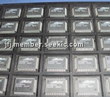
Product Summary
The A40MX04PQ100 is an FPGA. It offers a cost-effective design solution at 5V. The device is a single-chip solution and provides high performance while shortening the system design and development cycle. The A40MX04PQ100 can integrate and consolidate logic implemented in multiple PALs, CPLDs, and FPGAs. Example applications of the A40MX04PQ100 include high-speed controllers and address decoding, peripheral bus interfaces, DSP, and coprocessor functions.
Parametrics
A40MX04PQ100 absolute maximum ratings: (1)VCC DC Supply Voltage: –0.5 to +7.0 V; (2)VI Input Voltage: –0.5 to VCC+0.5 V; (3)VO Output Voltage: –0.5 to VCC+0.5 V; (4)tSTG Storage Temperature: –65 to +150 ℃.
Features
A40MX04PQ100 features: (1)High Capacity: Single-Chip ASIC Alternative; 3,000 to 54,000 System Gates; Up to 2.5 kbits Configurable Dual-Port SRAM; Fast Wide-Decode Circuitry; Up to 202 User-Programmable I/O Pins; (2)High Performance: 5.6 ns Clock-to-Out; 250 MHz Performance; 5 ns Dual-Port SRAM Access; 100 MHz FIFOs; 7.5 ns 35-Bit Address Decode.
Diagrams
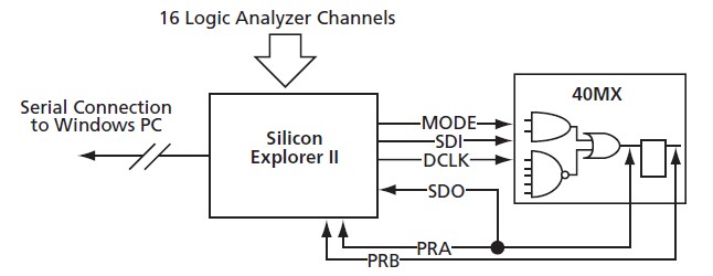
 |
 A40MX02 |
 Other |
 |
 Data Sheet |
 Negotiable |
|
||||||
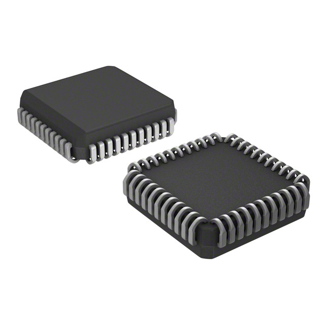 |
 A40MX02-1PL44 |
 |
 IC FPGA MX SGL CHIP 3K 44-PLCC |
 Data Sheet |

|
|
||||||
 |
 A40MX02-1PL44I |
 |
 IC FPGA MX SGL CHIP 3K 44-PLCC |
 Data Sheet |

|
|
||||||
 |
 A40MX02-1PL44M |
 |
 IC FPGA MX SGL CHIP 3K 44-PLCC |
 Data Sheet |

|
|
||||||
 |
 A40MX02-1PL68 |
 |
 IC FPGA MX SGL CHIP 3K 68-PLCC |
 Data Sheet |

|
|
||||||
 |
 A40MX02-1PL68I |
 |
 IC FPGA MX SGL CHIP 3K 68-PLCC |
 Data Sheet |

|
|
||||||
 (Hong Kong)

