(Hong Kong)

Product Summary
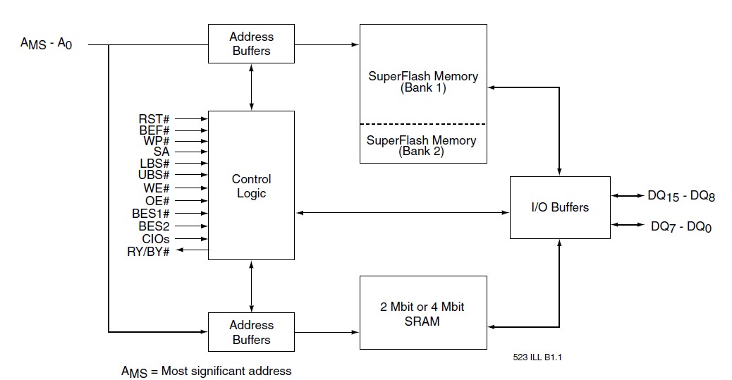
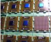
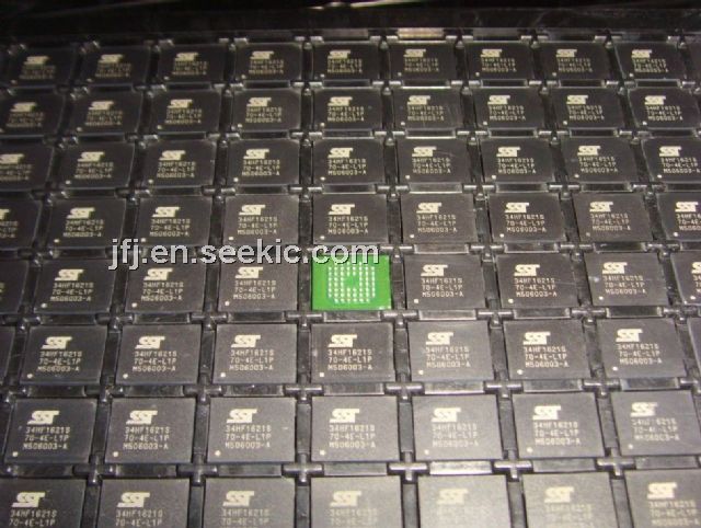
The SST34HF1621S-70-4E-L1P is a CMOS flash memory bank with a 256K x8/ 128K x16 or 512K x8/ 256K x16 CMOS SRAM memory bank in a Multi-Chip Package (MCP). The SST34HF1621S-70-4E-L1P is fabricated using SSTs proprietary, high-performance CMOS SuperFlash technology incorporating the split-gate cell design and thick oxide tunneling injector to attain better reliability and manufacturability compared with alternate approaches. The SST34HF1621S-70-4E-L1P is ideal for applications such as cellular phones, GPSs, PDAs and other portable electronic devices in a low power and small form factor system.
Parametrics
SST34HF1621S-70-4E-L1P absolute maximum ratings: (1)Operating Temperature: -20°C to +85°C; (2)Storage Temperature: -65°C to +125°C; (3)D. C. Voltage on Any Pin to Ground Potential: -0.5V to VDD 1+0.3V; (4)Transient Voltage (<20 ns)on Any Pin to Ground Potential: -1.0V to VDD 1+1.0V; (5)Package Power Dissipation Capability (Ta = 25°C): 1.0W; (6)Surface Mount Lead Soldering Temperature (3 Seconds): 240°C; (7)Output Short Circuit Current: 50 mA.
Features
SST34HF1621S-70-4E-L1P features: (1)Flash Organization: 1M x16; (2)Dual-Bank Architecture for Concurrent Read/Write Operation; (3)Single 2.7-3.3V Read and Write Operations; (4)Superior Reliability; (5)Low Power Consumption:; (6)Hardware Sector Protection: Protects 4 outer most sectors (4 KWord)in the larger bank by holding WP# low and unprotects by holding WP# high; (7)Hardware Reset Pin (RST#): Resets the internal state machine to reading data array; (8)Sector-Erase Capability; (9)Automatic Write Timing: Internal VPP Generation; (10)End-of-Write Detection; (11)CMOS I/O Compatibility; (12)JEDEC Standard Command Set; (13)Conforms to Common Flash Memory Interface (CFI).
Diagrams