(Hong Kong)

Product Summary
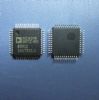
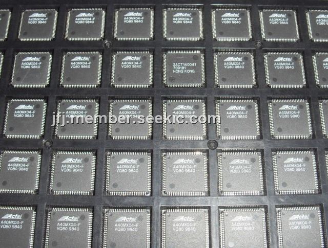
The A40MX04-FVQ80 is an FPGA. It offers a cost-effective design solution at 5V. The device is a single-chip solution and provides high performance while shortening the system design and development cycle. The A40MX04-FVQ80 can integrate and consolidate logic implemented in multiple PALs, CPLDs, and FPGAs. Example applications of the A40MX04-FVQ80 include high-speed controllers and address decoding, peripheral bus interfaces, DSP, and coprocessor functions.
Parametrics
A40MX04-FVQ80 absolute maximum ratings: (1)VCC DC Supply Voltage: –0.5 to +7.0 V; (2)VI Input Voltage: –0.5 to VCC+0.5 V; (3)VO Output Voltage: –0.5 to VCC+0.5 V; (4)tSTG Storage Temperature: –65 to +150 ℃.
Features
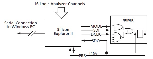
A40MX04-FVQ80 features: (1)High Capacity: Single-Chip ASIC Alternative; 3,000 to 54,000 System Gates; Up to 2.5 kbits Configurable Dual-Port SRAM; Fast Wide-Decode Circuitry; Up to 202 User-Programmable I/O Pins; (2)High Performance: 5.6 ns Clock-to-Out; 250 MHz Performance; 5 ns Dual-Port SRAM Access; 100 MHz FIFOs; 7.5 ns 35-Bit Address Decode.
Diagrams
| Image | Part No | Mfg | Description |  |
Pricing (USD) |
Quantity | ||||||
|---|---|---|---|---|---|---|---|---|---|---|---|---|
 |
 A40MX04-FVQ80 |
|
IC FPGA MX SGL CHIP 6K 80-VQFP |
Data Sheet |
|
|
||||||
| Image | Part No | Mfg | Description | |
Pricing (USD) |
Quantity | ||||||
 |
A40MX02 |
Other |
|
Data Sheet |
Negotiable |
|
||||||
 |
A40MX02-1PL44 |
|
IC FPGA MX SGL CHIP 3K 44-PLCC |
Data Sheet |
|
|
||||||
|
A40MX02-1PL44I |
|
IC FPGA MX SGL CHIP 3K 44-PLCC |
Data Sheet |
|
|
||||||
|
A40MX02-1PL44M |
|
IC FPGA MX SGL CHIP 3K 44-PLCC |
Data Sheet |
|
|
||||||
|
A40MX02-1PL68 |
|
IC FPGA MX SGL CHIP 3K 68-PLCC |
Data Sheet |
|
|
||||||
|
A40MX02-1PL68I |
|
IC FPGA MX SGL CHIP 3K 68-PLCC |
Data Sheet |
|
|
||||||