(Hong Kong)

Product Summary
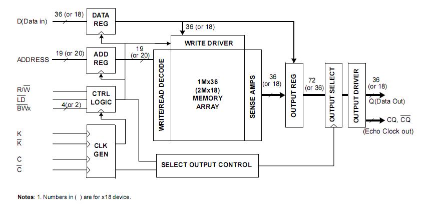
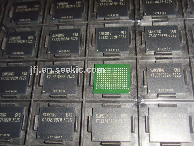
The K7J321882M-FC25 is a 37,748,736-bits DDR Separate I/O Synchronous Pipelined Burst SRAM. The K7J321882M-FC25 is organized as 1,048,576 words by 36bits for K7J323682M and 2,097,152 words by 18 bits for K7J321882M. The K7J321882M-FC25 is implemented with SAMSUNG high performance 6T CMOS technology and is available in 165pin FBGA packages.
Parametrics
K7J321882M-FC25 absolute maximum ratings: (1) Voltage on VDD Supply Relative to VSS: -0.5 to 2.9V; (2) Voltage on VDDQ Supply Relative to VSS: -0.5 to VDDV; (3) Voltage on Input Pin Relative to VSS: -0.5 to VDD +0.3V; (4) Storage Temperature: -65 to +150°C; (5) Operating Temperature: 0 to 70°C; (6) Storage Temperature Range Under Bias: -10 to +85°C.
Features
K7J321882M-FC25 features: (1) 1.8V+0.1V/-0.1V Power Supply; (2) DLL circuitry for wide output data valid window and future freguency scaling; (3) Separate independent read and write data ports; (4) Synchronous pipeline read with self timed late write; (5) Registered address, control and data input/output; (6) Byte write (x18, x36) function; (7) Simple depth expansion with no data contention; (8) 165FBGA(11x15 ball aray FBGA) with body size of 15x17mm.
Diagrams