(Hong Kong)

Product Summary
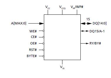
The PC28F512P33BF is an asynchronous, uniform block, parallel NOR Flash memory device manufactured on 65nm multilevel cell (MLC) technology. READ, ERASE, and PROGRAM operations are performed using a single low-voltage supply. Upon power-up, the PC28F512P33BF defaults to read array mode. The main memory array is divided into uniform blocks that can be erased independently so that valid data can be preserved while old data is purged.
Parametrics
PC28F512P33BF absolute maximum ratings: (1)Temperature under bias TBIAS: -50 to 125℃; (2)Storage temperature TSTG: -65 to 150℃; (3)Input/output voltage VIO: -0.6 to VCC +0.6V; (4)Supply voltage VCC: -0.6 to 4 V; (5)Input/output supply voltage VCCQ: -0.6 to 4 V; (6)Program voltage VPPH: -0.6 to 14.5V.
Features
PC28F512P33BF features: (1)Gb = stacked device (two 1Gb die); (2)Supply voltage, VCC = 2.7-3.6V (program, erase, read); VCCQ = 1.65-3.6V (I/O buffers); (3)Asynchronous random/page read, Page size: 16 words or 32 bytes; (4)Page access: 25ns; Random access: 100ns (Fortified BGA); 10ns (TSOP); (5)Buffer program: 512-word program buffer; (6)Program time, 0.88μs per byte (1.14 MB/s) TYP when using full 512-word buffer size in buffer program; (7)Memory organization, Uniform blocks: 128-Kbytes or 64-Kwords each; (8)Program/erase controller, Embedded byte/word program algorithms; (9)Program/erase suspend and resume capability, Read from any block during a PROGRAM SUSPEND operation; Read or program another block during an ERASE SUSPEND operation; (10)BLANK CHECK operation to verify an erased block; (11)Unlock bypass, block erase, chip erase, and write to buffer capability, Fast buffered/batch programming; Fast block/chip erase.
Diagrams
| Image | Part No | Mfg | Description |  |
Pricing (USD) |
Quantity | ||||||
|---|---|---|---|---|---|---|---|---|---|---|---|---|
 |
 PC28F512P33BF0 |
|
IC FLASH 512MBIT 95NS 64EZBGA |
Data Sheet |
Negotiable |
|
||||||
 |
PC28F512P33BFD |
|
IC FLASH 512MBIT P33 65NM 64BGA |
Data Sheet |
|
|
||||||