(Hong Kong)

Product Summary
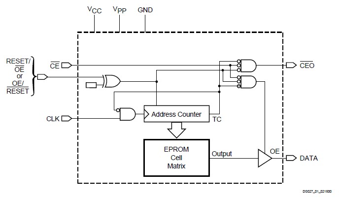
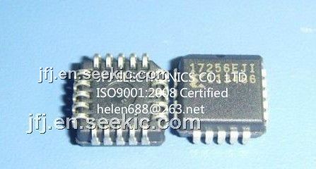
The XC17256EJI is a configuration PROM. It provides an easy-to-use, cost-effective method for storing large Xilinx FPGA configuration bitstreams. When the FPGA is in Master Serial mode, the XC17256EJI generates a configuration clock that drives the PROM. A short access time after the rising clock edge, data appears on the PROM DATA output pin that is connected to the FPGA DIN pin. Once configured, the XC17256EJI disables the PROM. When the FPGA is in Slave Serial mode, the PROM and the FPGA must both be clocked by an incoming signal.
Parametrics
XC17256EJI absolute maximum ratings: (1)VCC Supply voltage relative to GND: –0.5 to +7.0 V; (2)VPP Supply voltage relative to GND: –0.5 to +12.5 V; (3)VIN Input voltage relative to GND: –0.5 to VCC +0.5 V; (4)VTS Voltage applied to High-Z output: –0.5 to VCC +0.5 V; (5)TSTG Storage temperature (ambient): –65 to +150 ℃; (6)TSOL Maximum soldering temperature (10s @ 1/16 in.): +260 ℃.
Features
XC17256EJI features: (1)One-time programmable (OTP) read-only memory designed to store configuration bitstreams of Xilinx FPGA devices; (2)Simple interface to the FPGA; requires only one user I/O pin; (3)Cascadable for storing longer or multiple bitstreams; (4)Programmable reset polarity (active High or active Low) for compatibility with different FPGA solutions; (5)XC17128E/EL, XC17256E/EL, XC1701 and XC1700L series support fast configuration; (6)Low-power CMOS Floating Gate process; (7)XC1700E series are available in 5V and 3.3V versions; (8)XC1700L series are available in 3.3V only.
Diagrams