(Hong Kong)

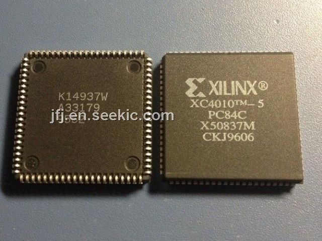
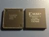
Product Summary
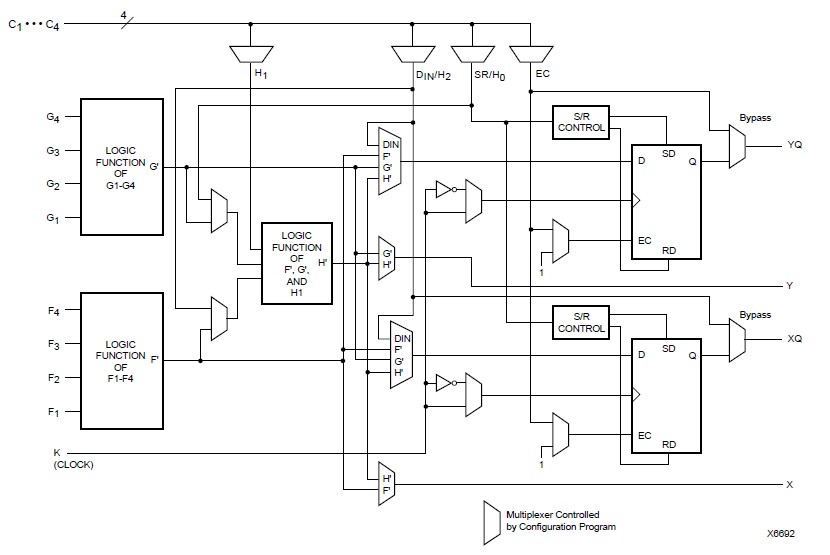
The XC4010-5PC84C is a high-performance, high-capacity Field Programmable Gate Array. The XC4010-5PC84C provides the benefits of custom CMOS VLSI, while avoiding the initial cost, long development cycle, and inherent risk of a conventional masked gate array. The result of fifteen years of FPGA design experience and feedback from thousands of customers, the XC4010-5PC84C combines architectural versatility, on-chip Select-RAM memory with edge-triggered and dual-port modes, increased speed, abundant routing resources, and new, sophisticated software to achieve fully automated implementation of complex, high-density, high-performance designs.
Parametrics
XC4010-5PC84C absolute maximum ratings: (1)High Performance-3.3 V XC4000XL; (2)High Capacity-Over 180,000 Usable Gates; (3)5 V tolerant I/Os on XC4000XL; (4)0.35μm SRAM process for XC4000XL; (5)Additional Routing Over XC4000E: almost twice the routing capacity for high-density designs; (6)Buffered Interconnect for Maximum Speed Blocks; (7)Improved VersaRing I/O Interconnect for Better Fixed Pinout Flexibility; (8)12 mA Sink Current Per XC4000X Output.
Features
XC4010-5PC84C features: (1)System featured Field-Programmable Gate Arrays: Select-RAMTM memory: on-chip ultra-fast RAM with Synchronous write option and Dual-port RAM option; Flexible function generators and abundant flip-flops; Dedicated high-speed carry logic; Internal 3-state bus capability; Eight global low-skew clock or signal distribution networks; (2)System Performance beyond 80 MHz; (3)Low power Segmented Routing Architecture; (4)Systems-oriented Features: IEEE 1149.1-compatible boundary scan logic support; Individually programmable output slew rate; programmable input pull-up or pull-down resistors; 12 mA sink current per XC4000E output; (5)Read Back Capability: Program verification and internal node observability.
Diagrams