(Hong Kong)

Product Summary
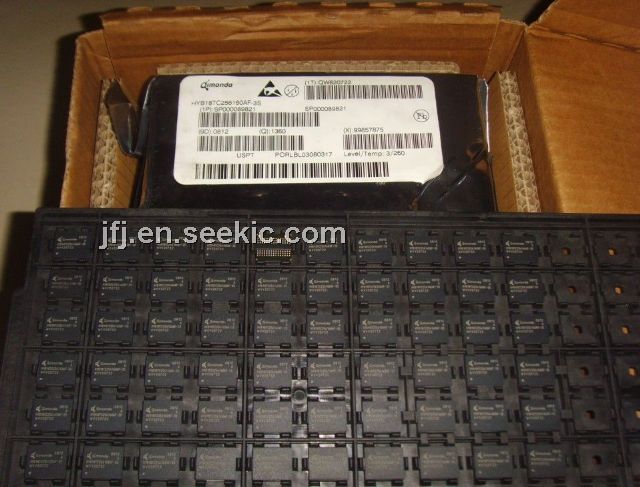
The HYB18TC256160AF-3S is a high-speed Double-Data-Rate-Two CMOS Synchronous DRAM device. The HYB18TC256160AF-3S contains 268,435,456 bits and internally configured as a quad-bank DRAM. The 256-Mbit HYB18TC256160AF-3S is organized as either16 Mbit×4 I/O ×4 banks, 8 Mbit×8 I/O ×4 banks or 4 Mbit ×16 I/O ×4 banks chip. The HYB18TC256160AF-3S acheives high speed transfer rates starting at 400Mb/sec/pin for general
applications.
Parametrics
HYB18TC256160AF-3S absolute maximum ratings: (1) Voltage on VDD pin relative to VSS, VDD: -1 to +2.3V; (2) Voltage on VDDQ pin relative to VSS, VDDQ: -0.5 to +2.3V; (3) Voltage on VDDL pin relative to VSS,VDDL: -0.5 to +2.3V; (4) Voltage on any pin relative to Vss, VIN, VOUT: -0.5 to +2.3V; (5) Storage Temperature Tstg: -55 to +100°C.
Features
HYB18TC256160AF-3S features: (1) 1.8 V±0.1 V Power Supply 1.8V ±0.1V (SSSTL_18) compatible I/O; (2) DRAM organizations with 4, 8 and 16 data in/outputs; (3) Double-Data-Rate-Two architecture: two data transfers per clock cycle four internal banks for concurrent operation; (4) Data masks (DM) for write data; (5) Off-Chip-Driver impedance adjustment (OCD) and On-Die-Termination (ODT) for better signal quality; (6) Auto-Precharge operation for read and write bursts; (7) Auto-Refresh, Self-Refresh and power saving Power-Down modes; (8) Full and reduced Strength Data-Output Drivers.
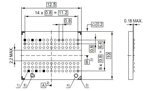
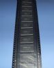
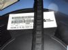
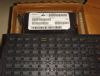
Diagrams