(Hong Kong)

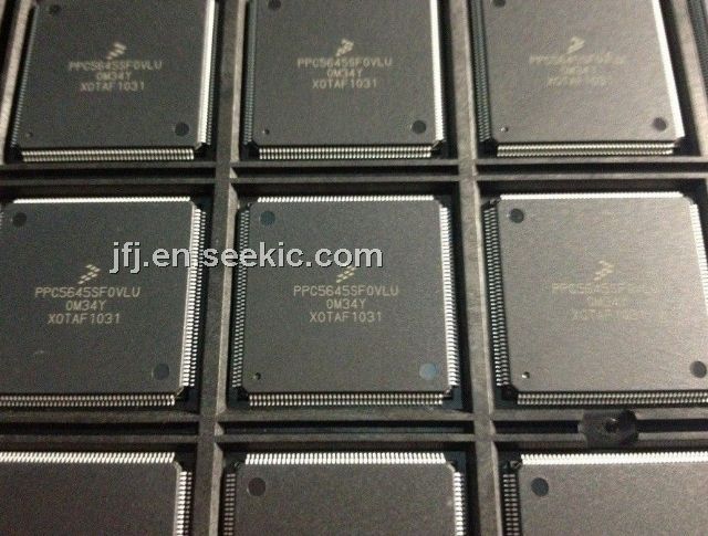

Product Summary
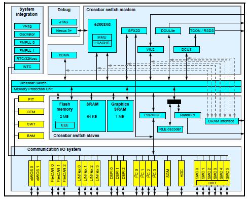
The PPC5645SFOVLU is a 32-bit microcontroller targeted single-chip automotive instrument cluster applications. The PPC5645SFOVLU is a part of the MPC56xxS family of Power Architecture based devices. This family has been designed with an emphasis on providing cost-effective and high quality graphics capabilities in order to satisfy the increasing market demand for color Thin Film Transistor (TFT) displays within the vehicle cockpit. Traditional cluster functions, such as gauge drive, real time counter, and sound generation are also integrated on each device.
Parametrics
PPC5645SFOVLU absolute maximum ratings: (1)VDDA, Voltage on VDDA pin (ADC reference) with respect to ground (VSSA): -0.3 to +5.5 V; Relative to VDD: VDD–0.3 to VDD+0.3V; (2)VSSA, Voltage on VSSA (ADC reference) pin with respect VSS: VSS–0.1 VSS+0.1 V; (3)VDDPLL, Voltage on VDDPLL (1.2 V PLL supply) pin with; (4)respect to ground (VSSPLL): 1.08 1.4 V D1.3; Relative to VDD: VDD–0.3 to VDD+0.3V; (5)VDDR, Voltage on VDDR pin (regulator supply) with respect to ground (VSSR): -0.3 +5.5 V; Relative to VDD: VDD–0.3 to VDD+0.3V; (6)VSSR, Voltage on VSSR (regulator ground) pin with respect to VSS: VSS–0.1 TO VSS+0.1 V; (7)VDD12, Voltage on VDD12 pin with respect to ground (VSS12): 1.08 to 1.4 V; (8)VSS12 CC D Voltage on VSS12 pin with respect to VSS: VSS–0.1 VSS+0.1 V; (9)VDDE_A, Voltage on VDDE_A (I/O supply) pin with respect to ground (VSSE_A): -0.3 +5.5 V; (10)VDDE_B, Voltage on VDDE_B (I/O supply) pin with respect to ground (VSS): -0.3 +3.6 V.
Features
PPC5645SFOVLU features: (1)Dual-issue, 32-bit Power Architecture Book E compliant CPU core complex (e200z4d); (2)Memory Management Unit (MMU); (3)4 KB, 2/4-way instruction cache; (4)2 MB on-chip ECC flash memory with:; (5)Flash memory controller; (6)Prefetch buffers; (7)64 KB on-chip ECC SRAM; (8)1 MB on-chip non-ECC graphics SRAM with two-port graphics SRAM controller; (9)Memory Protection Unit (MPU) with up to 16 region descriptors and 32-byte region granularity to provide basic memory access permission and ensure separation between different codes and data; (10)Interrupt Controller (INTC) with 181 peripheral interrupt sources and eight software interrupts; (11)Two Frequency-Modulated Phase-Locked Loops (FMPLLs); (12)Primary FMPLL (FMPLL0) provides a system clock up to 125 MHz; (13)Auxiliary FMPLL (FMPLL1) is available for use as an alternate, modulated or non-modulated clock source to eMIOS modules, QuadSPI and as alternate clock to the DCU and DCU-Lite for pixel clock generation; (14)Crossbar switch architecture enables concurrent access of peripherals, flash memory or RAM from multiple bus masters.
Diagrams