(Hong Kong)

Product Summary
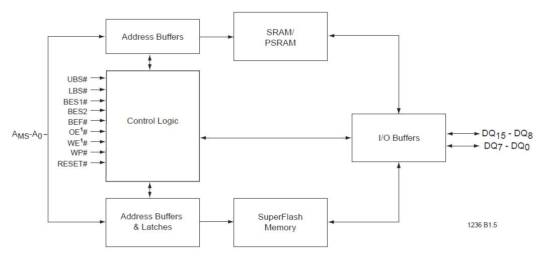
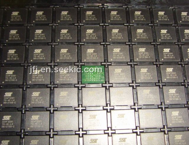
The SST32HF3281-70-4E-LS is a CMOS flash memory bank with a CMOS SRAM memory bank in a Multi-Chip Package (MCP), manufactured with SSTs proprietary, high performance SuperFlash technology. The SST32HF3281-70-4E-LS uses a PseudoSRAM. The SST32HF16x1C/32x1C devices use standard SRAM. The SST32HF3281-70-4E-LS consists of two independent memory banks with respective bank enable signals. The Flash and SRAM memory banks are superimposed in the same memory address space.
Parametrics
SST32HF3281-70-4E-LS absolute maximum ratings: (1)Operating Temperature: -20°C to +85°C; (2)Storage Temperature: -65°C to +150°C; (3)D. C. Voltage on Any Pin to Ground Potential: -0.5V to VDD 1+0.3V; (4)Transient Voltage (<20 ns)on Any Pin to Ground Potential: -1.0V to VDD 1+1.0V; (5)Package Power Dissipation Capability (TA = 25°C): 1.0W; (6)Surface Mount Solder Reflow Temperature: 260°C for 10 seconds; (7)Output Short Circuit Current: 50 mA.
Features
SST32HF3281-70-4E-LS features: (1)Single 2.7-3.3V Read and Write Operations; (2)Concurrent Operation: Read from or Write to SRAM while Erase/Program Flash; (3)Superior Reliability; (4)Low Power Consumption: Active Current: 15 mA (typical)for Flash or SRAM Read; (5)Flexible Erase Capability; (6)Erase-Suspend/Erase-Resume Capabilities; (7)Latched Address and Data for Flash; (8)Flash Fast Erase and Word-Program:; (9)Flash Automatic Erase and Program Timing: Internal VPP Generation; (10)Flash End-of-Write Detection; (11)CMOS I/O Compatibility; (12)JEDEC Standard Command Set; (13)Package Available; (14)All non-Pb (lead-free)devices are RoHS compliant.
Diagrams