(Hong Kong)

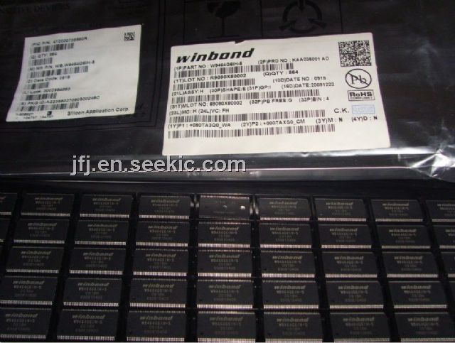
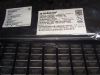
Product Summary
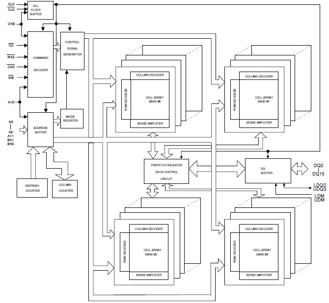
The W9464G6IH-5 is a CMOS Double Data Rate synchronous dynamic random access memory (DDR SDRAM); organized as 1M words × 4 banks × 16 bits. The W9464G6IH-5 delivers a data bandwidth of up to 500M words per second (-4). To fully comply with the personal computer industrial standard, the W9464G6IH-5 is sorted into the following speed grades: -4, -5, -5I, -6 and -6I. The -4 is compliant to the DDR500/CL3 and CL4 specification. By having a programmable Mode Register, the system can change burst length, latency cycle, interleave or sequential burst to maximize its performance. W9464G6IH is ideal for any high performance applications.
Parametrics
W9464G6IH-5 absolute maximum ratings: (1)Voltage on I/O Pins Relative to VSS VIN, VOUT: -0.5 ~ VDDQ +0.5 V; (2)Voltage on Input Pins Relative to VSS VIN: -1 ~ 3.6 V; (3)Voltage on VDD Supply Relative to VSS VDD: -1 ~ 3.6 V; (4)Voltage on VDDQ Supply Relative to VSS VDDQ: -1 ~ 3.6 V; (5)Operating Temperature (-4/-5/-6)TOPR: 0 ~ 70 °C; (6)Operating Temperature (-5I/-6I)TOPR: -40 ~ 85 °C; (7)Storage Temperature TSTG: -55 ~ 150 °C; (8)Soldering Temperature (10s)TSOLDER: 260 °C; (9)Power Dissipation PD: 1 W; (10)Short Circuit Output Current IOUT: 50 mA.
Features
W9464G6IH-5 features: (1)2.5V ±0.2V Power Supply for DDR 333/400; (2)2.6V ±0.1V Power Supply for DDR500; (3)Up to 250 MHz Clock Frequency; (4)Double Data Rate architecture; two data transfers per clock cycle; (5)Differential clock inputs (CLK and CLK ); (6)DQS is edge-aligned with data for Read; center-aligned with data for Write; (7)CAS Latency: 2, 2.5, 3 and 4; (8)Burst Length: 2, 4 and 8; (9)Auto Refresh and Self Refresh; (10)Precharged Power Down and Active Power Down; (11)Write Data Mask; (12)Write Latency = 1; (13)15.6μS Refresh interval (4K/64 mS Refresh); (14)Maximum burst refresh cycle: 8; (15)Interface: SSTL_2; (16)Packaged in TSOP II 66-pin, using Lead free materials with RoHS compliant.
Diagrams